Laser systems for micromaterial processing
InnoLas Solutions develops highly efficient machine solutions for the electronics, semiconductor and photovoltaic industries from innovations in laser technology. Thanks to a modular platform concept, each of our laser systems can be individually configured for the respective production task and designed as a stand-alone machine or for inline integration.
Solutions for the electronics and semiconductor industry
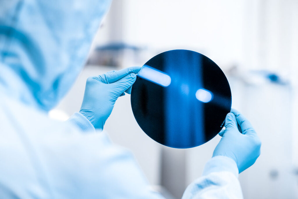
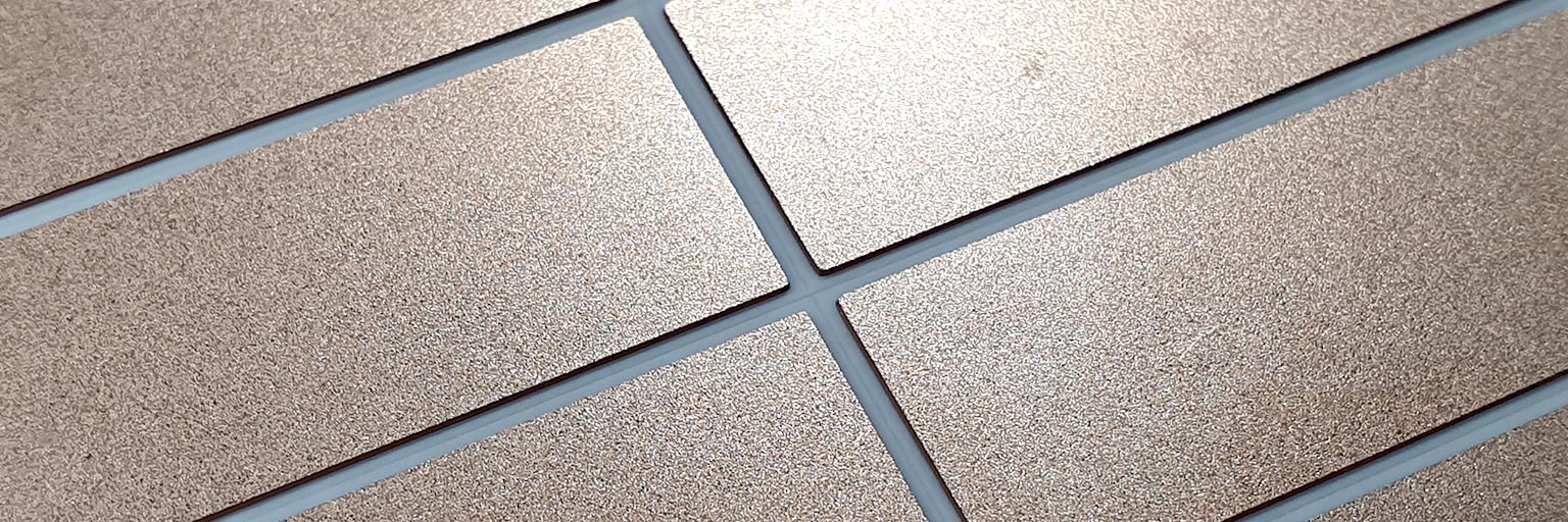
InnoLas Solutions develops highly efficient machine solutions for electronics production from innovations in laser technology. The use of ultrashort pulse lasers ensures optimum processing results when drilling, scribing, cutting and structuring PCB materials, ceramic substrates and semiconductor wafers.
PCB depaneling with the laser
Fast, economical and without residues
Depaneling of rigid as well as flexible printed circuit boards (PCBs) with state-of-the-art laser technology from Innolas Solutions is completely residue-free and ensures maximum material savings and low scrap rates thanks to full-cut and dense component arrangement.
Laser drilling with laser machines from InnoLas Solutions
PCB drilling with the laser from 2 µm in diameter
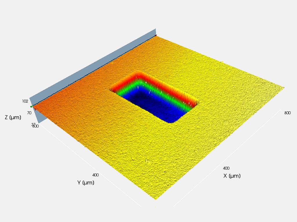
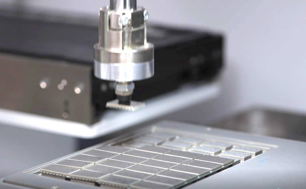
Laser drilling is one of our specialties. In order to process micro materials in electronic components down to the finest depths and diameters, we rely on ultrashort pulse lasers (UKP). The processes are melt-free and do not require any post-processing.
Your career at InnoLas Solutions
We are growing and looking for new energetic employees!
You too can come on board and write the success story with us as the world market leader in laser micromachining!

