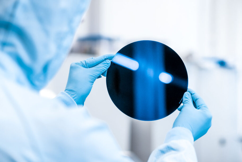
Cavity creation
At the cutting edge of tomorrow's technology

Electronic end devices are becoming smaller and smaller, and the space on the circuit boards is correspondingly becoming more and more precious. For a long time now, it has no longer been sufficient to equip the outer layers conventionally; instead, the inner layers are now also used. This is done by creating cavities during the production of the printed circuit boards. But what are cavities?
Cavities are small cavities that allow components to be accommodated in the inner layers of a printed circuit board, thus allowing increasingly complex assemblies to be accommodated in a smaller space. By creating several layers, so-called multilayers, the space can be maximally utilized in the same area.
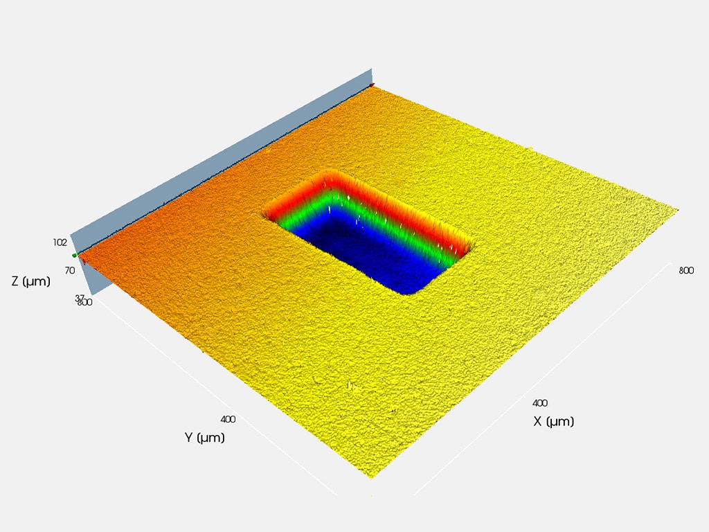
In order to place microchips, heat sinks, resistors and other components on the circuit boards, recesses known as cavities are made in the circuit board by means of lasers, whereby the excess material is removed. To do this, the laser first opens the copper surface and then removes the dielectric. Another laser pass cleans the exposed structure of the inner copper surface from resin residues. What sounds simple in theory requires the highest precision and reliable repeatability in practice.
Advantages of using lasers for cavities in printed circuit boards
If cavities in printed circuit boards are created with a laser system, this results in numerous advantages over other processes:
- Precise control of ablation depth and geometry of thecavity in contrast to conventional processes.
- High surface quality guaranteed with minimal thermal stress on the material (using suitable laser sources in the high-frequency range with pulse lengths in the picosecond range)
- CAD data and laser parameters are individually and highly precisely adapted to the different requirements
- The free etching of copper masks is unnecessary
- The process enables multiple cavities with different depths on changing design structures on a single PCB
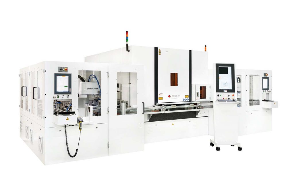
Cavities with laser machines from InnoLas Solutions
InnoLas Solutions is the market leader in laser processing of printed circuit boards of any material with a precision class of up to +- 5 µm.
We supply the right machine for every processing and manufacturing process. A choice of laser options and different system features depending on the application, allows you to find the right balance between cost and quality for your applications.
InnoLas Solutions is the right partner for both special applications and large series. We will be happy to support you in selecting the perfect solution for you:
- Laser sources:ultraviolet, green and infrared lasers with pulse durations in the nanosecond and picosecond range.
- Substrate size:small and large working areas covering all standard formats up to 30 x 30 inches
- Degree of automation:Stand-alone or as part of a fully integrated production line (Industry 4.0-capable)
Advantages of using lasers for cavities in printed circuit boards
Creating cavities using a laser system is not only more precise than with a conventional system, but also more economical. Thanks to the uncomplicated set-up of the system and the easy operability of the software, long setup times are eliminated. During production, the calibrated processes not only ensure significantly lower quality costs due to much higher accuracy, but also reduce the number of start-up parts and the reject rate. In addition, unlike a mechanical tool, a laser does not wear out, completely eliminating downtime for costly tool readjustment.
In addition, the laser systems from InnoLas Solutions are characterized by their versatility. A wide variety of processes are possible with our systems. In addition to the creation of cavities, depaneling, laser drilling or structuring of printed circuit boards are possible – and in some cases even simultaneously!
Technical Cleanliness
With laser systems, cavities in printed circuit boards can be created not only extremely economically, but also very cleanly. Unlike mechanical processes, laser processing does not generate dust that could contaminate the workpiece. The use of ultrashort pulse lasers also reliably prevents the formation of melt residues, as the material removed evaporates without leaving any residue. The vapors can be easily extracted.
The use of ultrashort pulse lasers also eliminates the additional step of free etching a copper mask into the surface of the PCB, as is necessary with processes using CO2 lasers. This in turn saves time and, in addition, no environmentally harmful chemicals are produced as waste.
No carbonization thanks to UKP lasers
InnoLas Solutions’ lasers operate in the femto- and picosecond range. Such lasers are called ultrashort pulse lasers (or UKP lasers for short). UKP lasers are characterized not only by the fact that they work with incomparable precision, but are also particularly gentle on the workpiece. With this technique, the input of thermal energy into the workpiece is reduced to such an extent that it has no relevant effect on the material properties. At just 30 to 50 °C, the heat input is far below that of the subsequent soldering processes. This gentle, layer-by-layer ablation of the material makes the process 100 percent carbonization-free.
Frequently asked questions about the use of lasers for cavities in printed circuit boards
At what point is a laser system economical?
Of course, this always depends on the individual case, but laser systems are significantly cheaper today than they were a few years ago. In addition, laser processing is no longer “only” superior to mechanical processes in terms of quality and quantity of production, but also in terms of cost. The elimination of mechanical machining processes not only avoids contamination, but also wear processes on tools. This eliminates all the time-consuming processes involved in cleaning the workpieces and readjusting the system. Furthermore, InnoLas Solutions’ laser systems are capable of running several processes simultaneously.
A laser system is therefore practically always worthwhile. If you still have doubts, just contact us – we will be happy to advise you individually.
With which technical interfaces are the InnoLas Solutions laser systems compatible?
Quite simply: with the one you want. Our equipment is fully Manufacturing Execution System (MES) compatible. That’s why the integration of our Industry 4.0-capable equipment into your fully integrated production line can easily be done via all common interfaces (SMEMA, Hermes, etc.). If, on the other hand, you need a special solution, this is no problem either, as we are able to implement a connection via all the interfaces you require. We will be happy to advise you on this in detail.
What is an ultrashort pulse laser?
An ultrashort pulse laser (UKP laser) works with laser pulses that are particularly short compared to other techniques such as the widely used CO2 laser. Namely, these are pulses in the picosecond and femtosecond range. A picosecond is the time period of a trillionth of a second, a femtosecond is even a quadrillionth of a second. To illustrate: While light travels a distance of 300,000 km in one second, it is just 0.3 mm in one picosecond and even only 0.3 nm in one femtosecond.
These extremely short pulses ensure that the material layers removed from the workpiece evaporate without leaving any residue and, moreover, that no carbonization occurs on the workpiece.
I need a laser system for a special application. Is there a solution for this?
As a matter of course. Since our foundation, we have not only offered equipment for large-scale production, but also for special applications. Our systems can be easily adapted according to the needs of our customers. This applies to the adaptation to the substrate size and the degree of automation as well as with regard to the selection of the laser. We supply you with the system that is best suited for your application.