Structuring printed circuit boards
Fast, economical and without residues

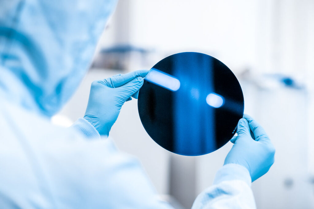
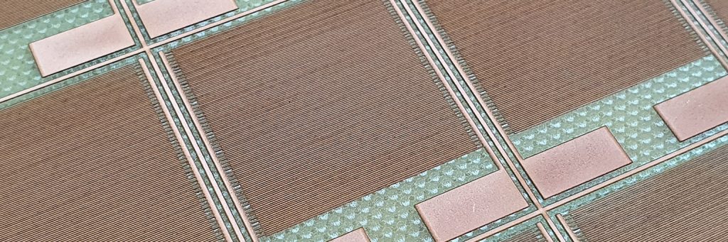
Laser structuring is a non-contact and wear-free process in which a pulsed laser beam is used to briefly and locally heat the material to be processed to such a high temperature that the corresponding part of the coating vaporizes. In this thermal process, the heat input to the board is not significant. For this reason, laser structuring is a particularly gentle and fast process with which even the most complex surface structures and the finest microstructuring can be implemented without any problems.
In the case of printed circuit boards, laser structuring has been used for almost 20 years to define electronic traces directly on the surface of the board in series production. Thanks to this stable and reliable process, smartphones, hearing aids, medical devices and sensors, for example, are becoming smaller and more powerful, while at the same time allowing complex and flexible geometric shapes and designs of all kinds, and all without the use of masking and etching processes.
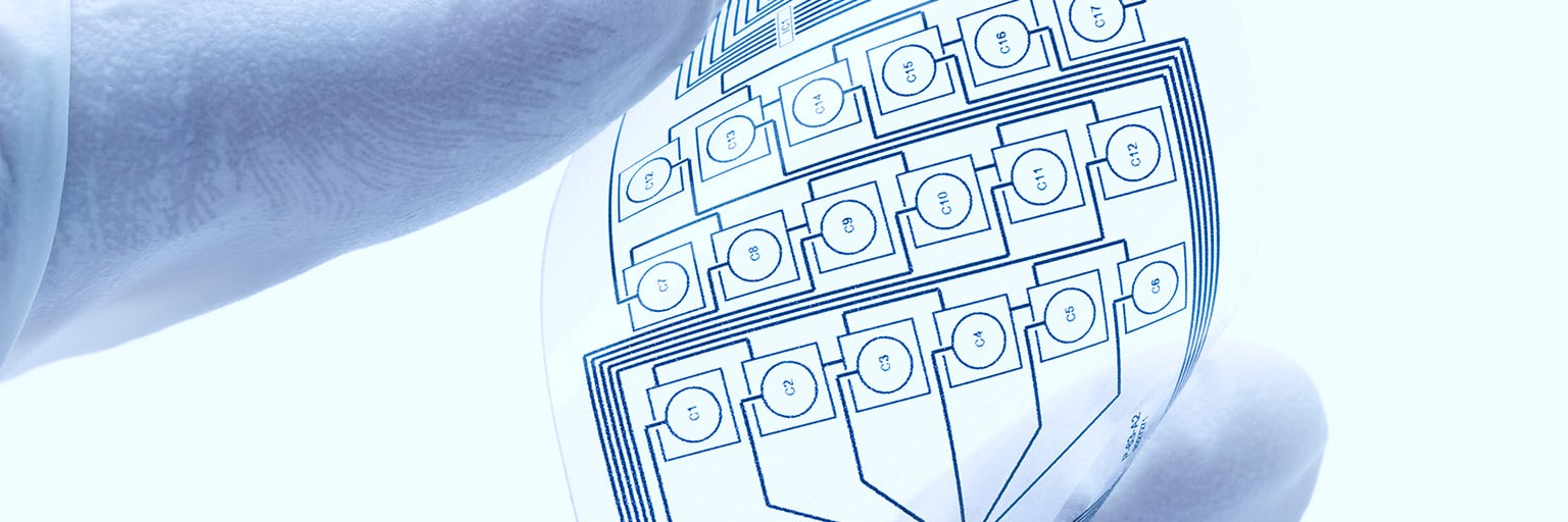
With our next-generation, state-of-the-art CAD-driven laser process, we can create traces in single- and double-sided, rigid and flexible PCBs, multilayers and high-performance circuits in minutes.
Our high-speed lasers achieve scan rates of up to 50 m per second, with positioning accuracy within 10 µm.
Laser structuring allows the pad diameter on the PCB to be reduced from 300 to less than 100 µm and the pad pitch of the components to be reduced to 0.3 m.
Advantages of laser structuring compared to alternative methods
Laser structuring offers numerous advantages over the classic masking and etching processes:
- Laser structuring of the copper top layer of printed circuit boards with minimal damage to the underlying material(dielectric)
- Very fine structures of less than 10 µm can be produced with high precision and repeatability.
- The mapping of exact geometries on a wide variety of materials is easily possible (e.g. FR4, aluminum-coated PET films, ceramics, etc.).
- The number of conventional process steps is reduced while at the same time increasing flexibility in geometry
- Environmentally harmful materials and residues are significantly reduced – this not only improves environmental protection, but also reduces disposal costs
- Unlimited editing of layouts
- Economical and efficient
Structuring with laser machines from InnoLas Solutions
InnoLas Solutions is the market leader in structuring printed circuit boards of any material with a precision of up to +/- 5 µm.
We supply the right machine for every processing and manufacturing process. A choice of laser options and different system features depending on the application, allows you to find the right balance between cost and quality for your applications.
InnoLas Solutions is the right partner for both special applications and large series. We will be happy to help you choose the perfect solution for you:
- Laser sources:ultraviolet, green and infrared lasers with pulse durations in the nanosecond and picosecond range.
- Substrate size:small and large working areas covering all standard formats up to 30 x 30 in.
- Degree of automation:Stand-alone or as part of a fully integrated production line (Industry 4.0-capable)
High degree of automation
Thanks to their SMEMA standard design, InnoLas Solutions laser systems can be easily automated with all systems from leading automation manufacturers. Or to put it another way: our plants are of course Industry 4.0-capable. This ensures that all relevant information on the status of the plant is always available in real time. This facilitates optimized control of the production network. However, with our systems you always remain flexible, because they are available both as stand-alone and integrated into an inline solution.
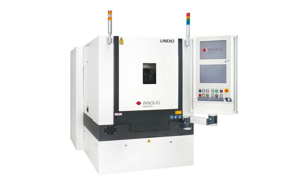
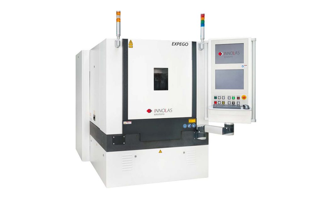
The plants themselves also feature a high degree of automation. For example, our products in the LINEXO and EXPEGO series each have
- an automatic camera calibration,
- Programs for plant referencing and process control
- a vision system for component registration and
- an automatic correction of offset, rotation, size and keystone distortion.
This reduces sources of error and guarantees consistent quality. The resulting high process stability noticeably reduces scrap compared to conventional processes.
Advantages of InnoLas Solutions laser systems
Isn’t laser structuring very expensive? We are still frequently asked this question and we can only ever give the same answer: No, lasering is not expensive. The initial cost of a system for laser structuring of conductor plates may be somewhat higher than that for a comparable system for an etching or milling process, but even if this should be the case, the costs are usually recouped in a relatively short time. This is because laser systems not only allow selective and targeted ablation of thin layers to expose the electrically conductive tracks, but also enable production at significantly higher speeds.
Environmentally friendly production by means of laser structuring
Even today, the majority of ladder boards are manufactured by giving their surface its structure in a photochemical process. The resulting chemical waste pollutes people and the environment. However, environmental protection is becoming an increasingly important issue in the industry. More and more consumers are asking themselves under what conditions the electrical appliances they use were produced. This makes the environmental balance of production a USP in its own right. Laser processing scores particularly well in this respect. In contrast to conventional etching processes, this technology contributes significantly to reducing chemical waste from manufacturing.
Save time with laser structuring
When you choose a laser scribing system from InnoLas Solutions, you save – above all – time, which in turn is worth hard cash.
- You save training time, because thanks to our user-friendly software your employees quickly find their way around the new system
- You save set-up time, because all our systems are characterized by short set-up times
- You save working time that you would otherwise need for readjusting mechanical parts, e.g. in milling processes
To put it in a nutshell: The acquisition costs of a laser system can currently still be somewhat higher than those for a conventional one. However, the non-contact and thus (almost) wear-free machining and the high process stability significantly reduce operating costs – while at the same time improving quality.
Frequently asked questions about laser structuring
Can laser systems perform multiple work steps?
Yes! Depending on the model, the laser systems from InnoLas Solutions can be used not only for structuring but also for marking, drilling, creating cavities, and cutting.as is required, for example, for depaneling. Even in these applications, a laser system achieves accuracy and speed far beyond those of conventional processes. The InnoLas Solution systems are even capable of running the relevant processes in parallel.
What other methods are there for structuring printed circuit boards?
The most widely used processes worldwide are still photochemical processes, in which a layer of photosensitive lacquer is exposed on the metallic conductor plate through a mask and then etched accordingly. This process not only leads to the environmental impact already mentioned, but also delays production because the components cannot be processed elsewhere during the process. With laser structuring, on the other hand, there is no chemical waste and other work steps can be carried out simultaneously during structuring.
A process used primarily in the manufacture of prototypes is milling. In this process, layers of copper are mechanically structured. This process naturally causes metal dust and chips on the workpiece, and the milling head also wears out quickly and therefore requires regular readjustment. This also causes considerable loss of time and waste. A laser system, on the other hand, vaporizes the coating without leaving any residue.
For which applications are the InnoLas Solutions laser systems suitable?
Our laser systems are suitable for a wide range of applications in almost all areas of the electrical industry. We are one of the leading suppliers of laser systems for absolutely residue-free and carbonization-free
depaneling
. If scoring of the same is desired before the final separation of the utility, we of course have a solution for that as well. Furthermore, our systems are suitable for laser drilling of micro vias with high aspect ratios and diameters up to 15 µm. In order to accommodate the increasing miniaturization of modern electronic devices and their printed circuit boards, we also offer comprehensive solutions in the area of
generation of cavities
are available.
Of course, you will find all these solutions combined in just one laser system. In some cases, the individual processes can even be executed in parallel. Only laser cutting systems are this extensive and efficient!
A process used primarily in the manufacture of prototypes is milling. In this process, layers of copper are mechanically structured. This process naturally causes metal dust and chips on the workpiece, and the milling head also wears out quickly and therefore requires regular readjustment. This also causes considerable loss of time and waste. A laser system, on the other hand, vaporizes the coating without leaving any residue.
Which lasers are used for structuring?
Our facilities exclusively use ultrashort pulse lasers in the femto- and picosecond range in the ultraviolet, green and infrared parts of the spectrum. As a result, the heat input to the workpiece is significantly lower than with previously used lasers, which worked with longer pulses. Thanks to these properties, it is ensured that the material to be removed evaporates without residues and that no carbonization occurs.
A process used primarily in the manufacture of prototypes is milling. In this process, layers of copper are mechanically structured. This process naturally causes metal dust and chips on the workpiece, and the milling head also wears out quickly and therefore requires regular readjustment. This also causes considerable loss of time and waste. A laser system, on the other hand, vaporizes the coating without leaving any residue.