Depaneling of printed circuit boards with the laser
Fast, economical, reliable and clean: laser depaneling

Increasing demands on printed circuit boards require new production methods in electronics manufacturing. InnoLas Solutions’ laser systems increase the quality and reliability of your products while reducing production costs.
Depaneling printed circuit boards with lasers has decisive advantages over conventional processes. Our lasers produce perfectly clean cut edges with no residue, dust or carbonization. Due to the possible elimination of pre-routing structures, considerably more assemblies can be arranged per panel in the full-cut process.
In addition, higher throughputs can be realized with laser cutting than with classic processes, since several processing units per machine work in parallel on one job.
This saves costs while improving quality.
Depaneling - taken to a whole new level
What are the advantages of laser depaneling compared to alternative manufacturing processes?
- In depaneling with lasers, several process units per machine work simultaneously. This allows processing timesto be significantly reduced compared to conventional production methods.
- Different processes can be carried out one after the other or in parallel, such as Cutting, Drilling or Structuring
- Material usage reduction – PCB material savings through PCB designs without pre-routing. In the full-cut process, the laser requires almost no PCB area in the processing zone (<0.5mm)
- No thermal energy input in the cutting zone, low “heat-affected zone” (HAZ) due to cold ablation
- High-precision cuts, highest cutting accuracies up to 5µm
- No mechanical stress or damage due to non-contact and vibration-free separation
- Reduction of failure rates in the end application; circuit reliability is significantly improved
- Reduction of cleaning effort and stable process conditions without any mold changes
- 100% technical cleanliness of the cutting edge
- Dust-free processing due todirect evaporation and suction of the material
- Flexibility and material diversity, we have the right laser for almost every material
- Complex cutting contours and small radii without additional setup times
- Technical cleanliness: carbonization-free processing, no burning of the material.
- 100% reproducible process quality through cross-machine and calibrated process parameters; also from machine to machine
- High and flexible level of automation from stand-alone to a fully integrated production line (Industry 4.0 capable) – Everything from a single source!
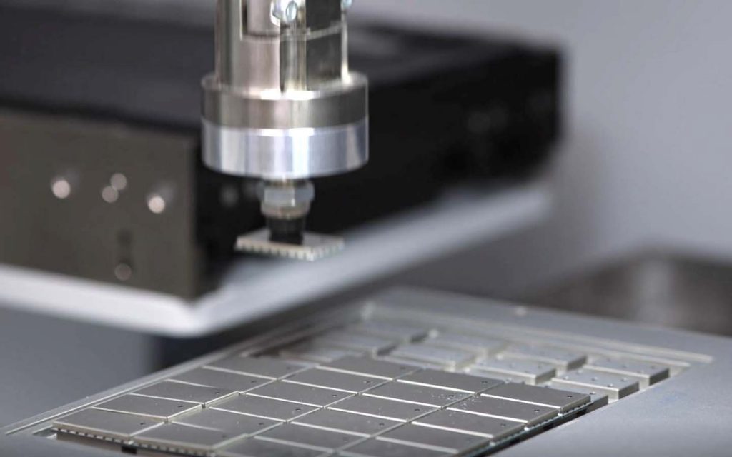
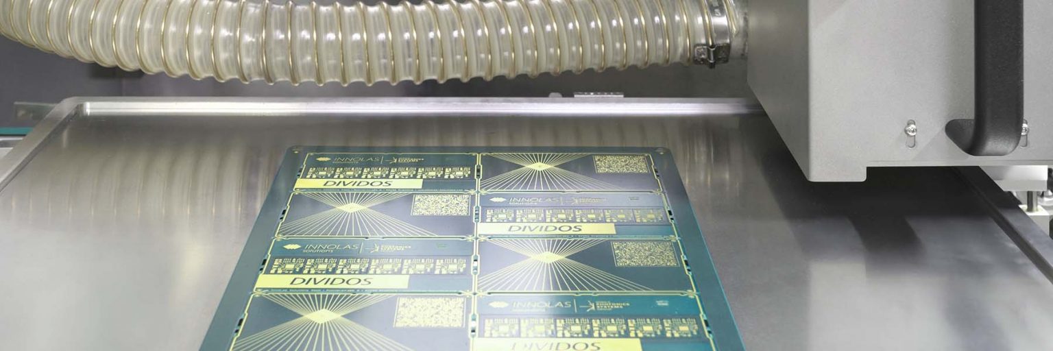
Depaneling with laser machines from InnoLas Solutions
InnoLas Solutions is the market leader in depaneling printed circuit boards of any material with a precision/accuracy of +- 5 µm. With over 2,000 systems worldwide, we are one of the most successful global players in the field of depaneling printed circuit boards.
With our highly flexible, modular plant concepts, we supply the right machine for every processing and manufacturing process. Whether you need stand-alone equipment or highly complex, fully automated production lines (including further process steps such as inspection or sorting), InnoLas Solutions is your one-stop shop.
A wide range of laser options and different system features depending on the application, allows you to find the right balance between cost and quality for your depaneling applications.
InnoLas Solutions is the right partner for both special applications and large series. We will be happy to assist you in choosing the perfect solution for you in view of our various options:
- Laser sources:Nano-, pico- or femptosecond lasers in the common wavelengths from IR to ultraviolet are standard with us.
- Substrate size: Modular plant concepts offer a suitable basic machine, regardless of the size of the substrate
- Degree of automation: a stand-alone or a fully integrated production line (Industry 4.0-capable) from a single source
Frequently Asked Questions about Laser Depaneling / Depaneling
Compared to mechanical cutting processes (milling, punching), InnoLas laser depaneling offers you many economic advantages:
- Fast production processes, more throughput
- No changing or wearing out of tools
- Longer service life of the machine (freedom from wear)
- Less material loss due to more filigree contour guides and closer positioning – spacing between PCBs <0.5mm possible
- Less scrap due to contactless, vibration-free cutting and more stable processes
- Higher product quality and less waste, also in aftersales of end products
No, because with InnoLas Solutions laser depaneling solutions the heat input is not significant (HAZ/heat affection zone). We use ultra-short pulse lasers that do not heat the material. Instead of burning and forming soot, the material vaporizes directly in a quasi-cold process during benefit separation.
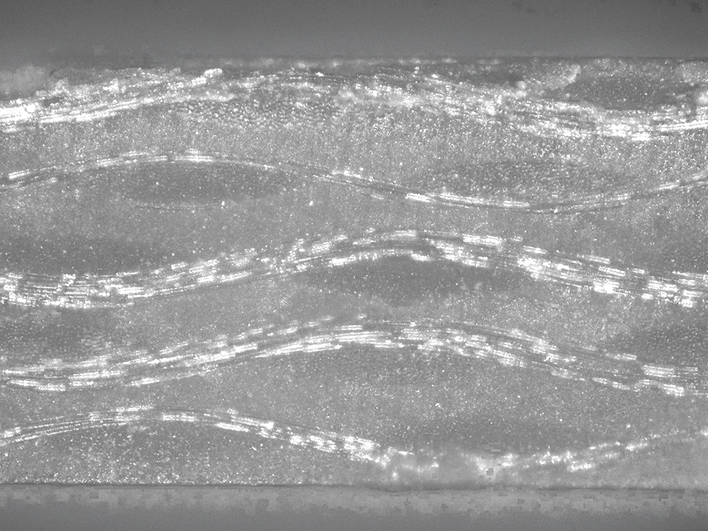
The cut edges are therefore absolutely clean and to 100% carbonation free. The temperature influence in the cutting area is only 30°-50°, i.e. lower than in the upstream soldering process.
On the contrary. Thanks to full automation with up to eight laser heads (multi-head system with Multi Beam Technology), many times the speed of a conventional milling system can already be achieved. Marking on-the-fly (MOF)” perfectly synchronizes the movement of the panel with the movement of the laser beam.
This saves an additional approx. 40% processing time.
The integration of an optimized scanner increases accuracy in machining and throughput in production, creating added value for the customer. The modular systems from InnoLas Solutions achieve +/- 5 µm accuracy. The overall processing of the pattern avoids stitching errors. Pulse on Demand (POD) also guarantees highly precise machining. Our machines thus control and regulate the amount of energy entered at each location of the components, regardless of the complexity of the layout. At the same time, throughput is increased because travel distances and subsequent calibration as well as downtimes are eliminated.
Classic methods for depaneling are cutting or scoring with wedge-shaped knives and cutting with the depaneling cutter or a saw. Depaneling with the laser is already an established process. Its advantages lie above all in the high production quality, the very precise and at the same time gentle material processing without carbonization or the like and the fast processing times in production.
Modern electrical appliances are getting smaller and smaller. This also shrinks the size of the printed circuit boards. At the same time, the functional scope of these devices is increasing. What is good for users, on the other hand, makes production enormously more difficult. To simplify production, several printed circuit boards are therefore combined to form a so-called panel. Several printed circuit boards are manufactured and assembled in large panels (also called panels). At the end of the manufacturing process, the individual printed circuit boards must be separated from the panel. This process is called depaneling.
When cutting PCB panels with a laser, the fully assembled PCBs are cut from a panel by a focused laser beam directly vaporizing the material layer by layer very quickly. In the process, lasers can very easily be used to create any desired ultra-fine structures. The vapors generated during the separation process are extracted, which also ensures that no deposits or residues remain on the finished product.
The price, of course, depends very much on the size and characteristics of each machine. However, today the laser machines are not much more expensive than a milling machine. In addition, the additional costs are usually quickly amortized by the elimination of wear parts and the higher production capacity. The calibrated processes also produce significantly fewer start-up parts and rejects. The price/performance ratio of laser cutting systems has improved by a factor of 10 over the past 10 years.